_1.png "Blog Header 2 (00000)_1")


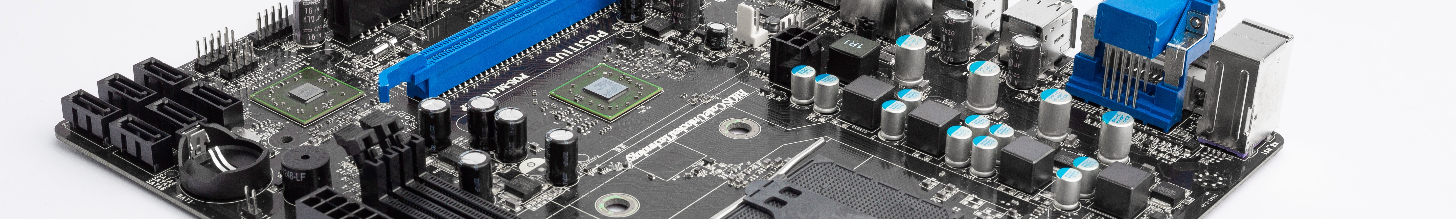
Advanced Packaging was developed to improve device performance while shrinking packages at the same time. It involves grouping a variety of distinct electronic packaging techniques including flip chip, CSP, system-in-package (SiP), system-on-package (SoC), package-on-package (PoP), 2.5D, 3D-IC, and FOWLP. By utilizing these packages, you can integrate different technologies which are ideally optimized for memory, radio frequency (RF), or power, and with that comes new challenges. As an example, the first mobile phones were a little under 23 mm thick. The sleek and stylish 10 mm phones of 2020 were only possible thanks to wafer-level packaging (WLP) and PoP.
Advancements are largely due to the advent of very large heterogeneous characteristics, also known as "integration". Heterogeneous integration allows for the packaging of components of different functionalities, different process technologies, and sometimes separate manufacturers.
While the technique of putting multiple chips in a package has been around for decades, the development and progress of advanced packaging are defined by Moore’s law which states “the number of transistors on a microchip doubles every 18 to 24 months”. Moore’s law scaling has been the primary focus of System-On-Chip packages over the last 50+ years. This has resulted in an industry-driven, device-level integration of several billion-transistor chips incorporating progressively more and more functions in a single die while reducing cost.
However, as Moore’s law is approaching its limits in combined scaling and cost reduction, there are unique opportunities for heterogeneous package integration to enable better devices in the short term and to enable better systems in the long term. Many applications such as RF devices, power management systems, biochips, sensors, and MEMS play a significant role in today’s semiconductor products. Without advanced packaging, there is no way the iPhone could shrink to the size it is today. In the future, packaging will be the technology that enables miniaturization and power efficiency. Making use of through-silicon vias (TSVs), interposers, bond wires, ball grid arrays, and other techniques, we can shrink the interconnects to reduce power consumption and increase power efficiency.
%20-%20Copy%20-%20Copy-jpg.jpeg?width=375&height=434&name=Matt%20Hands%20CU%20(00000)%20-%20Copy%20-%20Copy-jpg.jpeg)
These technological advancements are bringing a renewed focus on package and chip design, fabrication, and the manufacturing process. When it comes to advanced packaging, there is a renewed focus on the use of no-clean pastes/fluxes. The effect of no-clean flux residue on signal integrity is a concern for many RF and high-frequency products such as 5G and other communication products. No-clean flux residue can create an alternative path to the signal and degrade the signal integrity performance, especially at high frequencies. This is known as the Hall Effect or Skin Effect when the signals travel along the path of least resistance instead of going through the intended circuit. This results in leakage current and it can affect product performance. With increasing frequencies, we expect higher signal loss and signal wavelengths are continuously decreasing, requiring smaller circuit features, finer pitch components, and tighter spacing. These factors increase potential risks for cross-contamination and leakage issues – especially when the packages contain flux residues (including No-clean).
Advanced Packages involving heterogeneous integration will be impacted by the challenges posed by component miniaturization. The trend is towards smaller, thinner, lighter, denser, more reliable, and more functional devices. In short, the real estate on the package and/or chip is continuously shrinking and this has a direct impact on the solder paste/flux formulation used. With miniaturization advancing rapidly for advanced packages, the solder powder used in the paste materials needs to be finer, resulting in increased flux activity levels. As the pad size reduces, the oxygen penetration path through flux or solder paste also decreases resulting in more rapid oxidation of flux materials. Additional oxidation would demand more carboxylic acids in the flux thereby increasing the flux activity levels which will dictate the formulation of engineered chemical solutions needed to remove the residues quickly, effectively, and without compromising material compatibility. Additionally, this will also bring a renewed focus on the equipment capabilities in terms of spray nozzle configuration, spray impingement pressures, wash temperatures, MOCs, seals, and more.
